China chip industry growth fueled by AI packaging

Introduction to China’s Chip Industry
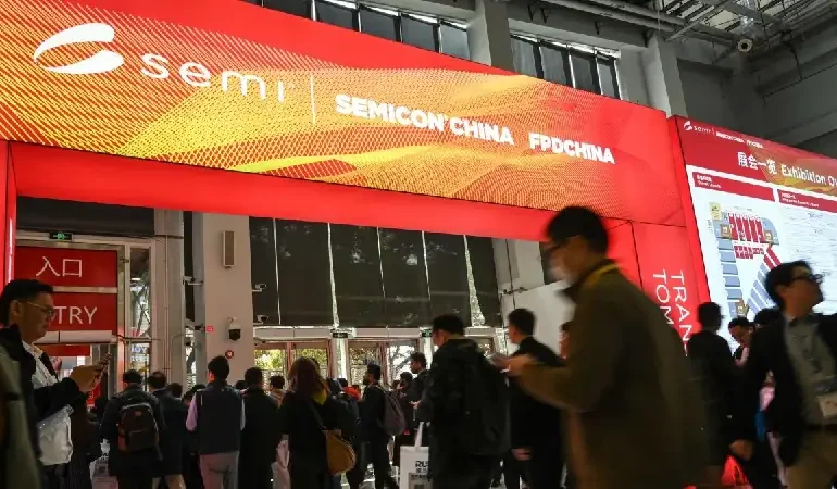
Semicon China’s message was blunt: the China chip industry is finding its next growth lane by marrying AI demand with packaging-led performance gains rather than waiting for a clean leap in leading-edge lithography. The event’s talk track centered on practical production wins—better yields, tighter cycle times, and more domestic substitution in tools and materials that matter to throughput. As reported by SCMP’s Semicon China coverage, exhibitors and executives framed 2025 orders around compute-heavy workloads and the back-end steps that turn wafers into usable products. That shift spotlights foundries, OSATs, and component suppliers that can ship now, not narratives about distant node parity. The growth case being sold is execution: make more chips, package them smarter, and move them into servers, phones, and vehicles at competitive cost.
Role of AI in Semiconductor Growth
AI in semiconductors is showing up less as marketing and more as a demand signal that changes purchasing patterns across the stack. Data-center builds need accelerators, high-bandwidth memory interfaces, fast interconnects, and power management that can survive sustained loads. That pulls capacity toward mature and specialty processes that are available at scale, while also raising the value of design services and EDA flows that shorten time to tape-out. The same AI boom is tightening memory and component pricing, which feeds into procurement decisions for OEMs and pushes suppliers to lock in longer contracts. For a view of how component inflation can ripple through downstream devices, see Xiaomi’s warning on memory costs. The upshot at Semicon China was that compute demand is real and immediate, so winners will be those who can deliver stable volumes, predictable power efficiency, and consistent reliability at shipment scale.
Advanced Packaging Technologies
Advanced chip packaging is being treated as a performance multiplier and a workaround for constrained access to the most advanced front-end tooling. The industry’s emphasis has shifted to integrating more capability at the package level: stacking, chiplets, denser substrates, improved thermal solutions, and tighter interconnect spacing to reduce latency and raise bandwidth. Packaging also changes the competitive map because it rewards process control, materials quality, and assembly precision—areas where incremental progress compounds quickly in yields and cost per usable unit. A fast-moving packaging ecosystem can also pull along domestic suppliers of substrates, bonding equipment, and inspection tools, broadening where value is captured. This matters for firms already pushing alternative architectures; Alibaba’s RISC-V chip effort illustrates how design choices can pair with packaging advances to target specific workloads. Semicon China’s takeaway was that back-end innovation is no longer secondary; it is a primary battleground for performance per dollar.
Global Market Impact
China semiconductor growth driven by AI and packaging has direct effects on trade, pricing, and supply-chain alignment. As domestic buyers prioritize secure and scalable supply, overseas vendors face tougher qualification hurdles and more pressure to localize service and support. At the same time, stronger Chinese output in mature nodes and packaged modules can add volume into global channels, influencing prices for commodity components and forcing rivals to differentiate on quality, power efficiency, and long-term availability. The packaging push also elevates materials and critical inputs—substrates, chemicals, specialty gases—where global competition is intense and procurement is increasingly strategic. Parallel moves by other regions to de-risk supply lines show how quickly the chessboard is shifting; the Australia-EU critical minerals deal is one example of upstream positioning. For manufacturers selling into export markets, growth will hinge on compliance, documentation, and customer confidence as much as on raw capacity numbers.
Future Projections and Challenges
The forward view presented around Semicon China was not a promise of effortless domination; it was an argument that scale, packaging sophistication, and AI-driven demand can keep utilization high while bottlenecks are addressed. The main challenges are operational and structural: securing enough high-quality materials, improving test and reliability data to meet global customer standards, and managing the cost curve as designs grow more complex. Advanced packaging can lower system costs, but it also adds new failure modes, thermal constraints, and inspection requirements that must be mastered to avoid expensive returns. Policy and export-control pressure remains a constant variable, shaping what equipment can be sourced and how quickly domestic alternatives can be validated. Broader trade resistance is already rising in multiple regions; developing markets tightening trade defenses underscores the environment chipmakers will sell into. The credible projection is continued growth through execution—higher yields, better packaging, and steady customer conversion—rather than a single headline technology leap.