
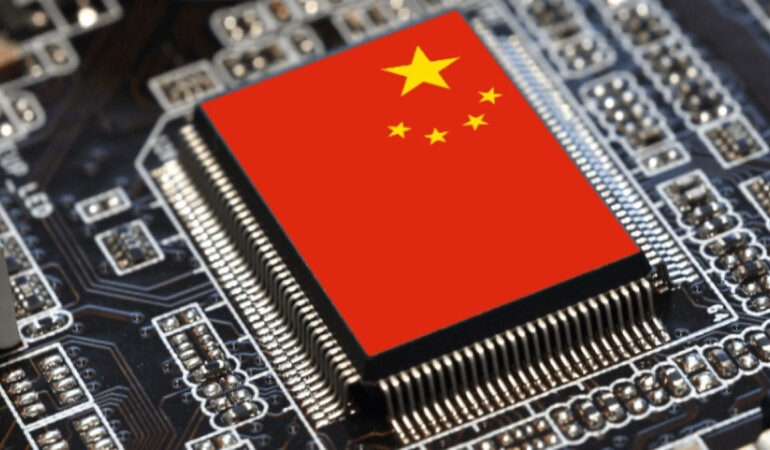
China Pushes for 50 Percent Domestic Fab Tools as Self Sufficiency Gaps Persist
China’s ambition to boost self sufficiency in wafer fabrication equipment is entering a more assertive phase, with industry sources indicating that new semiconductor fabs are being encouraged to source at least 50 percent of their tools from domestic suppliers. While the guideline has not been formalized in public regulations, companies seeking approval for new capacity are reportedly asked to demonstrate that half of their semiconductor production equipment spending goes to Chinese manufacturers.
The push comes as export controls have complicated access to advanced foreign tools. Semiconductor Manufacturing International Corp recently disclosed that some equipment it had procured in advance from overseas vendors could not be fully deployed because supporting systems were unavailable. The mismatch has left certain tools idle, underscoring the operational risks tied to sanctions and servicing restrictions.
China’s wafer fabrication equipment industry has made measurable progress in areas such as deposition, etching, cleaning and plating. Domestic suppliers including Naura Technology Group, Advanced Micro Fabrication Equipment and ACM Research have expanded revenue rapidly, supported by strong local demand and policy backing. Analysts estimate that China’s total spending on wafer fabrication tools exceeded 40 billion dollars last year and is expected to rise steadily through 2028, making the country one of the largest global markets for such equipment.
A growing portion of that spending is flowing toward domestic vendors rather than US, Japanese or Dutch suppliers. Substitution has been more feasible in non lithography segments where Chinese tools are considered increasingly competitive. However, lithography remains a critical bottleneck. Shanghai Micro Electronics Equipment can supply steppers for mature nodes such as 90 nanometers and above, but tools capable of sustaining high volume production at 28 nanometers or below remain limited.
Advanced immersion deep ultraviolet systems and extreme ultraviolet lithography machines, produced primarily by ASML, represent the most complex segment of the supply chain. These tools rely on highly specialized optics, materials and software ecosystems developed over decades. Industry observers caution that bridging this gap could take many years, even with significant state investment.
China’s strategy appears to balance flexibility with long term goals. Reports suggest that authorities may grant waivers for advanced nodes where domestic alternatives are not yet viable, while applying the 50 percent threshold more strictly to mature process lines. Measurement criteria can vary, whether by total value, number of chambers or specific tool categories, giving regulators room to adapt.
At the same time, Chinese fabs are working to localize components within domestically produced tools to reduce dependence on foreign subsystems. Export controls have accelerated efforts to qualify non US alternatives for pumps, controllers and other key parts. Although eliminating foreign content entirely remains complex, progress has been reported in reducing exposure to restricted components.
The broader question is whether accelerated localization can deliver tools that match international standards for yield, throughput and reliability at advanced nodes. While domestic capacity is expanding and government support remains firm, technological catch up in lithography and inspection systems continues to define the pace of China’s wafer fabrication self sufficiency drive.