
China Pushes Toward EUV Lithography as It Accelerates AI Chip Development
China is intensifying efforts to develop its own extreme ultraviolet lithography technology, a move that could significantly strengthen the country’s ambitions in advanced semiconductor manufacturing and artificial intelligence hardware. Reports that Chinese researchers and engineers are making progress toward building a domestic EUV lithography machine have drawn close attention, as the technology sits at the heart of producing the world’s most advanced chips.
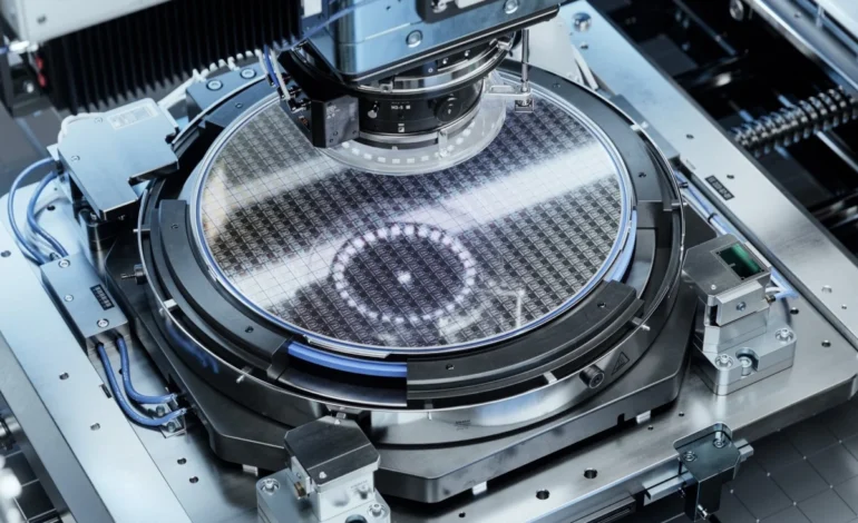
EUV lithography is widely regarded as one of the most complex and strategically important technologies in the global semiconductor industry. It allows chipmakers to etch extremely small and precise circuit patterns onto silicon wafers, enabling the production of cutting edge processors used in artificial intelligence, high performance computing and advanced data centers. At present, commercial EUV systems are dominated by a single supplier, the Dutch firm ASML, with exports tightly restricted under international controls.
For China, mastering EUV technology would represent a major breakthrough. Access to advanced lithography tools has become one of the biggest bottlenecks facing Chinese chipmakers as they attempt to move beyond mature manufacturing nodes. Without EUV, producing chips at the most advanced process levels becomes far more difficult, slower and less efficient. This has limited China’s ability to compete directly with leading global players in areas such as AI accelerators and high end processors.
Industry analysts say that even partial success in developing a domestic EUV system could provide China with a substantial strategic advantage. While building a fully comparable machine would take years of testing, refinement and supply chain coordination, progress alone would reduce dependence on foreign technology and help insulate the sector from external pressure. It would also signal that China is closing the gap in one of the most technically demanding areas of modern manufacturing.
The push for EUV capability fits into a broader national strategy focused on semiconductor self reliance. In recent years, Beijing has increased funding for chip research, equipment development and talent cultivation, viewing semiconductors as a foundation of economic security and technological competitiveness. Artificial intelligence has become a central driver of this strategy, with growing demand for powerful chips to support large models, industrial automation and scientific research.
Developing EUV lithography is not only a technical challenge but also an organizational one. The systems require advanced light sources, ultra precise optics, specialized materials and extremely clean manufacturing environments. Each component demands expertise across physics, engineering and materials science. Observers note that China’s strength in large scale industrial coordination may play a role in gradually overcoming these hurdles.
The implications of success would extend beyond China’s domestic market. Greater access to advanced chipmaking tools could reshape global semiconductor competition and alter supply chain dynamics, particularly in AI related hardware. It could also influence how other countries approach technology controls and cooperation.
While uncertainty remains around timelines and technical readiness, China’s determination to pursue EUV lithography highlights how central semiconductor capability has become to its long term technological goals. As AI continues to drive demand for more powerful and efficient chips, progress in this field could play a decisive role in shaping the next phase of global tech rivalry.