
Chinese Scientists Unveil Breakthrough Optical Computing Chip with Unprecedented Parallel Power
Chinese researchers have announced a major breakthrough with the creation of the world’s first ultra high parallel optical computing integrated chip. The chip delivers a theoretical peak performance of 2560 TOPS at a 50 GHz optical clock speed, putting it in direct comparison with some of the most advanced GPU chips on the market. This development marks a significant leap in computing technology as scientists explore ways to move beyond traditional electronic processors.
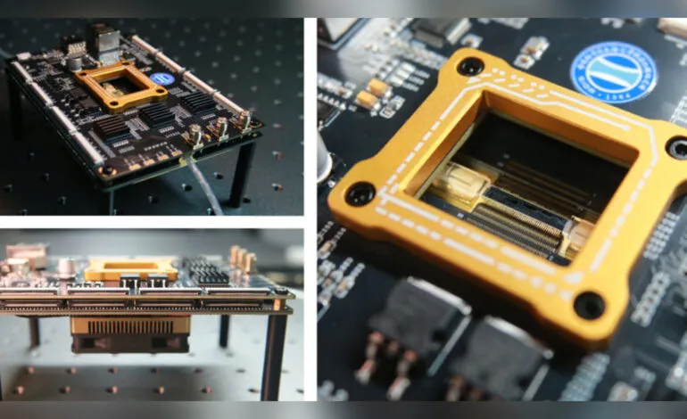
Innovation Led by the Shanghai Institute of Optics and Fine Mechanics
The achievement comes from a research team at the Shanghai Institute of Optics and Fine Mechanics under the Chinese Academy of Sciences. Their work introduces a new architecture for photonic computing that dramatically expands the possibilities of high speed information processing. By designing a chip with over 40 nanometers of bandwidth, low energy loss and fully reconfigurable functions, the team has created a platform capable of achieving far greater performance than earlier optical computing systems.
A central breakthrough lies in the integration of soliton microcomb sources. These generate more than 100 separate wavelength channels on a single chip, allowing large numbers of operations to occur at the same time. This approach represents a major step forward in the quest to build computing systems that can process vast volumes of data with extraordinary efficiency.
How Multi Wavelength Processing Changes the Game
Xie Peng, a researcher involved in the project, explained that the chip supports computation across more than 100 wavelength channels simultaneously. This creates an environment where information can be processed in dense parallel streams. Traditional optical computing techniques rely on a single wavelength, limiting speed and scalability. By contrast, the new chip’s architecture allows up to 100 times more computing power without increasing the physical size or operating frequency.
Engineer Han Xilin described the concept as turning a single lane road into a hundred lane highway. With many more channels open at once, the flow of information increases dramatically while the hardware remains compact. The result is a computing process that can handle complex workloads with greater speed and lower latency.
Transforming Future Technologies
Optical computing has long been seen as a promising direction for next generation processors due to its natural advantages in speed, parallelism and bandwidth. This new chip pushes that vision closer to mainstream adoption. The ability to pack so much computing power into a small footprint makes the architecture especially appealing for artificial intelligence applications, large scale data centers and advanced simulations.
The research team highlighted its potential impact on fields such as embodied intelligence, neural network processing, image recognition and scientific modeling. Low latency photonic systems are also well suited for edge devices, including communication nodes and drone fleets where rapid response is essential despite limited data volumes.
A Breakthrough Recognized by the Scientific Community
The team’s findings have gained significant attention and were published as a cover paper in the journal eLight under the title Parallel Optical Computing Capable of 100 Wavelength Multiplexing. The publication underscores the scientific importance of the achievement and its potential to reshape digital architecture. As research continues, the emergence of optical chips like this one may signal a new era in which computing systems become faster, more efficient and fundamentally different from the electronic hardware we rely on today.