
Semiconductor Labs Report Breakthroughs in Energy Efficient Chip Design
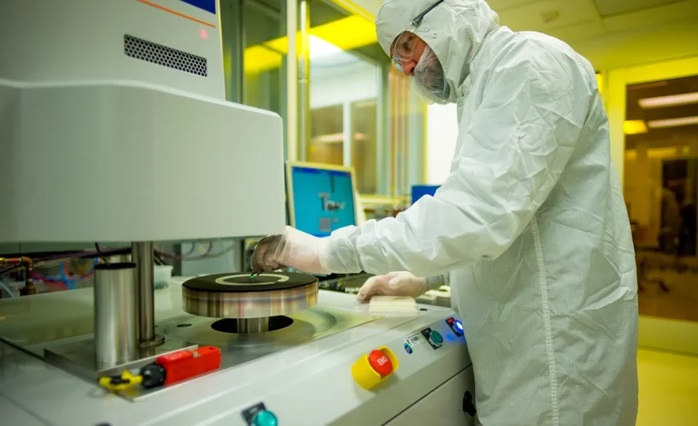
Semiconductor laboratories across China are announcing a series of breakthroughs in energy-efficient chip design, signalling a shift toward architectures that prioritise power optimisation alongside raw performance. As artificial intelligence models grow in size and complexity, and as edge devices demand higher compute density without excessive heat generation, the industry is increasingly focused on pushing the boundaries of energy efficiency. The latest research highlights how labs are exploring novel circuit layouts, advanced packaging methods, and redesigned memory systems to meet escalating computational demands while keeping power consumption under control. These developments reveal a broader trend in China’s semiconductor ecosystem as researchers target the next stage of chip evolution through power-aware engineering.
Reducing power consumption across core logic pathways
One of the key advancements unveiled by semiconductor labs involves the refinement of core logic pathways to reduce unnecessary switching activity, a major source of energy loss in integrated circuits. Engineers are testing new transistor arrangements, gate structures, and voltage control techniques that allow individual compute units to activate only when needed. This reduces static and dynamic power consumption without compromising performance.
Some labs have reported success with variable precision computing methods, which allow chips to adjust the precision of arithmetic operations based on workload requirements. This approach significantly lowers energy usage in AI workloads that do not always require maximum precision. Research teams are also experimenting with adaptive clocking systems that synchronise power delivery more precisely, helping chips maintain stable performance at lower voltage thresholds.
Memory innovation becomes a central priority
Energy-efficient design is not limited to compute cores. Memory systems, particularly high-bandwidth memory layers, represent one of the most energy-intensive components in modern chips. To address this challenge, labs are focusing on new high-density memory structures that reduce power leakage and improve data transfer efficiency. Some teams have developed early prototypes of memory architectures that shorten signal routing distances, reducing both latency and energy consumption.
Other advances include the integration of non volatile memory elements into accelerator chips, enabling data to be stored with lower power requirements and accessed more quickly. These enhancements are vital for training and inference tasks that require frequent movement of large datasets between memory units and processing clusters.
Progress in 3D packaging and thermal optimisation
Several semiconductor laboratories have also reported breakthroughs in three-dimensional packaging technologies, an area that has become increasingly important as chips incorporate more computing modules in tight spaces. Traditional two-dimensional layouts are reaching limits in terms of performance scaling and thermal management. Three-dimensional stacking allows chips to achieve higher compute density, but managing heat becomes more complex.
Researchers in China are experimenting with new thermal interface materials, improved heat dissipation pathways and optimised layer stacking strategies. These methods help distribute heat more evenly and reduce hotspots that can damage chip components. In some trials advanced cooling channels have been embedded directly into the packaging structure, providing greater thermal stability during high intensity workloads. Such innovations are critical for supporting next generation accelerators used in large scale AI and scientific computing.
Power efficiency as a competitive differentiator
As semiconductor competition intensifies globally, energy-efficient design is becoming a key differentiator for manufacturers and research labs. With restrictions limiting access to leading-edge fabrication equipment, Chinese researchers are focusing on architectural innovation and system-level optimisation as pathways to maintain competitiveness. Energy efficiency offers a strategic advantage because it enables chips to perform complex tasks within constrained thermal envelopes, making them suitable for both data center applications and edge scenarios.
Industry analysts note that global demand for energy efficient chips is rising rapidly as companies seek to reduce data center power consumption and improve sustainability metrics. Chinese labs view this trend as an opportunity to shape new markets by providing architectures optimised for efficiency rather than only for performance. If these breakthroughs can be translated into commercial products, Chinese semiconductor firms may gain traction in emerging markets that require compact, low power, high throughput processors.
Implications for AI systems and future research
Energy-efficient chip designs have far-reaching implications for the future of AI. Large language models and other deep learning systems require enormous computational resources, and improvements in energy efficiency help lower operational costs and reduce environmental impact. Efficient chips also enable more powerful AI capabilities on edge devices such as autonomous drones, smart appliances, and industrial robots.
The breakthroughs reported by Chinese semiconductor labs represent early steps toward a broader shift in chip design philosophy. As researchers continue to explore novel materials, innovative packaging techniques and adaptive computing frameworks, the industry appears to be entering a new stage driven by the dual priorities of performance and sustainability.